Microinstructions Guide
Remarks:
If you are struggling with microinstructions, or need more depth init, then refer to this document, i've written my thought process when going through any instruction for filling table
I've added images as well to avoid any typos (but if u find any typos pls reach out or point it on the discussion forum for COMP2280) (i hope there isn't any typos)
Lastly to strengthen ur understanding and gain confidence, practice these steps for all 16 instructions types OR untill u gain confidence (trust me it gets simple after 2, 3 instructions)
Feel free to reach out or ask any questions regarding it on discussion forum - Krish Sanjay Bhalala
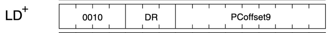
Instruction: LD R7 Label
-
In your instruction register of 16 bits these bits will be store 0010 111 000000001 assuming the label is at address PC+PCoffset9
-
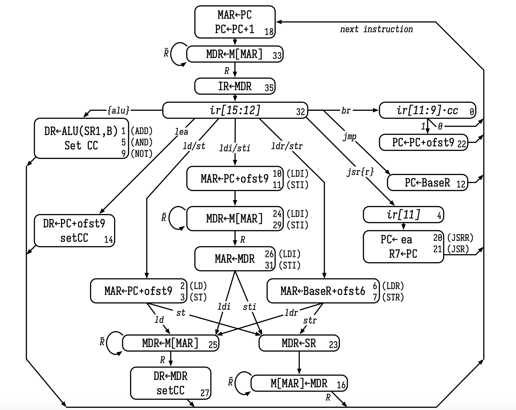
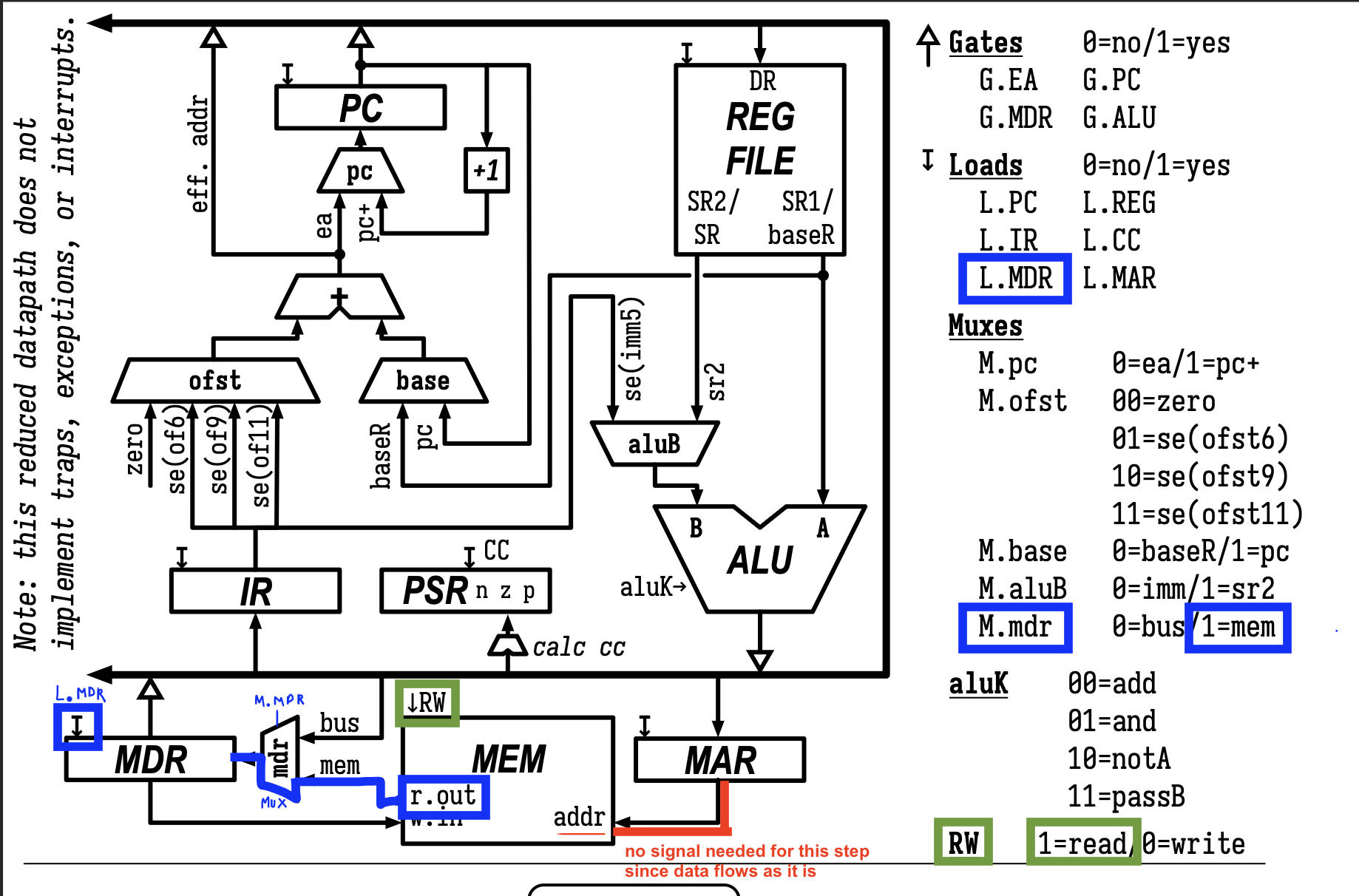
Now look at your state diagram and lc3 circuit diagram to figure out what signals to activate in your circuits and in what order
-
The signals that u activate for each state will go in single row of your reference table
-
-
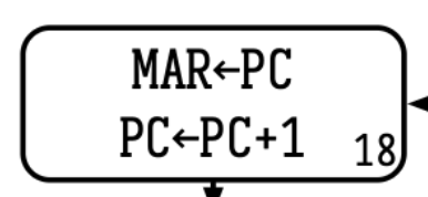
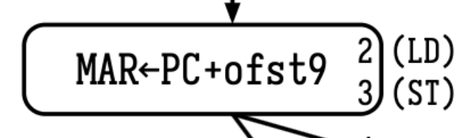
Lets start from a state (usually in exam they would give u the starting state) if not then simply start by 18
-
simply put in your start state and next state (in this case its 18 and 33 respectively)
-
for state 18 we are basically loading the PC into MAR and incrementing PC (this is kind of part of fetching instruction stage, as we are basically prepping for quering the memory for the instruction stored at address PC). Lets break down the state into more simpler steps
-
eg-
-
In this state we are doing a bunch of things in order
-
fetching the value of PC and bringing it to MAR
-
Updating the value of MAR with PC value
-
Incrementing and updating the PC value with PC+1
-
-
each of those steps would require specifc signals to be triggered.
-
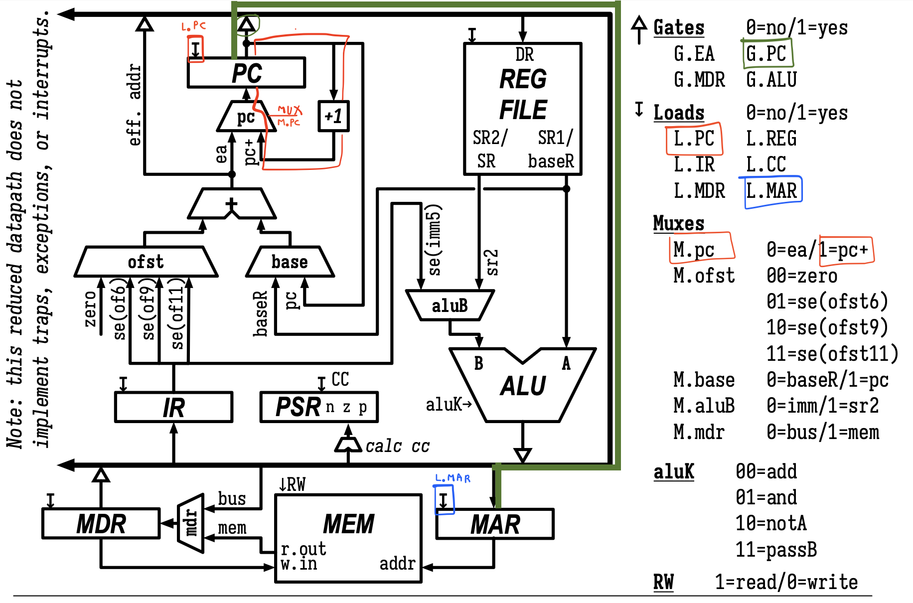
Now which signals to activate would depend on the components in the circuits being activated
-
Simply look at ur circuit diagrams (I've color code the steps to make it look more clear about what steps are triggering what signals)
-
-
-
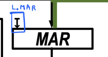
fetching the value of PC and bringing it to MAR
-
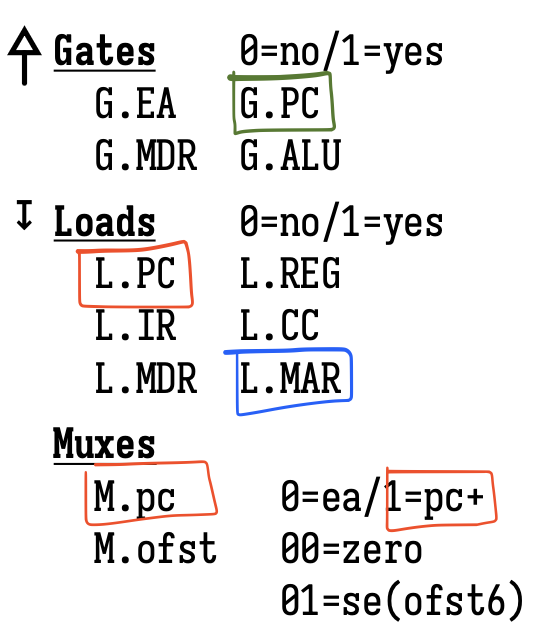
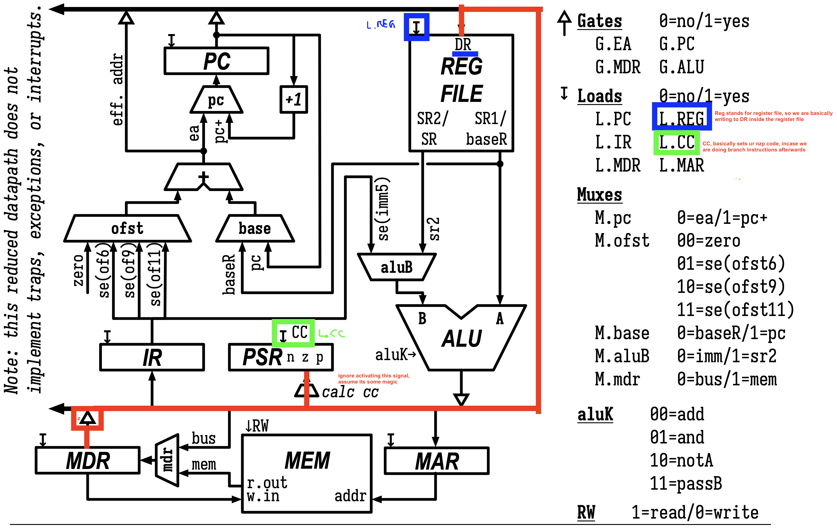
we need to bring the PC data into the MAR but its too far so we will use the bus, and whenever u want to use the bus you need, u need to use the gates (triangle things) to let the data flow into the bus, in this case we will use G.PC = 1 (basically saying open the gate of PC to let the data flow in bus)
-
-
Updating the value of MAR with PC value
-
since PC is already flowing in the bus we need to write it into the MAR register for this step (so we will use load signals for this to write data to registers) specifically we will set L.MDR = 1 (basically saying overwrite the data in MAR which the data recieved via the wire)
-
-
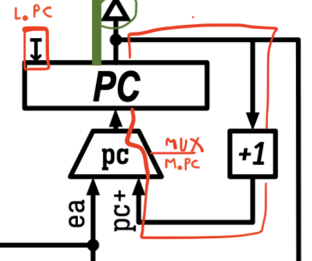
Incrementing and updating the PC value with PC+1
-
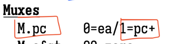
Now +1 represents literally adding +1 to PC so that box will output PC+1 and that flows directly to MUX with pc written on it which basically selects what value to write it PC. it has multiple inputs, but we are only interested in PC+1 so we set signal M.PC = 1 (basically its saying, select the line of PC+1 and let it pass through it)
-
Lastly we need to override that PC+1 data into PC register, which once again we will use good old signal load specifically L.PC = 1 (bascially it says whatever value that im recieveing from below, overwrite that into PC)
-
-
-
So at state 18 you are activating these signals
-
 which is exactly what you are filling it in your table with their values 1,0
-
-
-
-
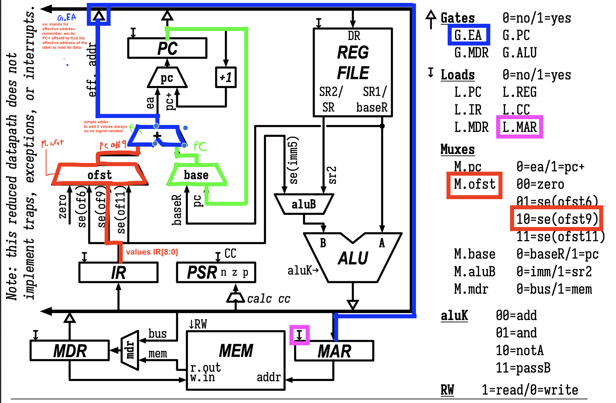
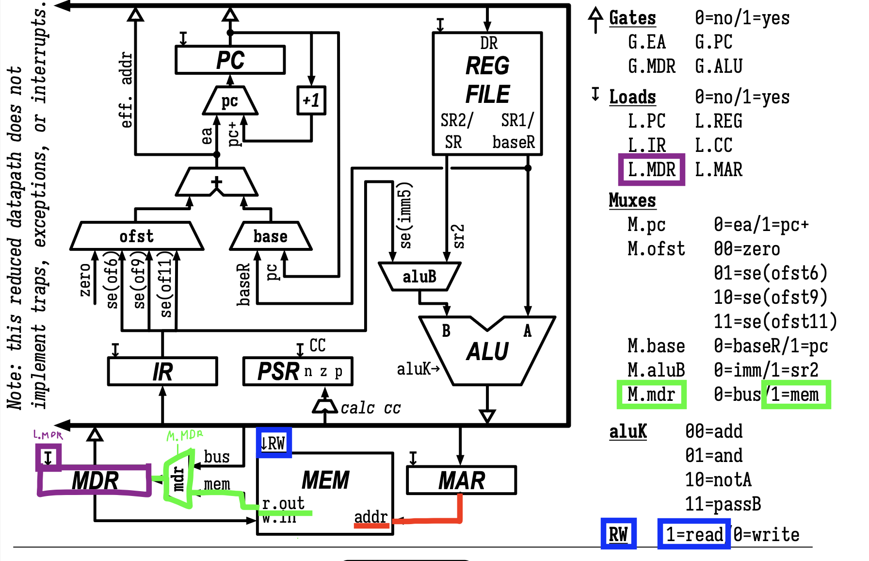
Next we move to step 33 based on the FSM
-
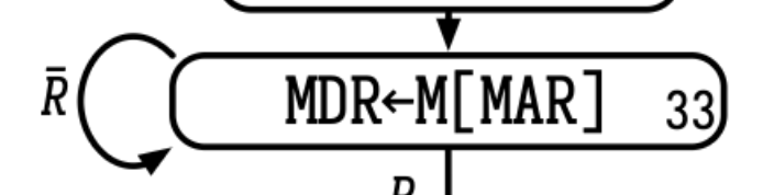 ignore the R transition
 -
here the steps are
-
bring the value of MAR into the memory M
-
no singals are needed as data is always flowing in those red wires anyways
-
-
Read the value at address stored in MAR in memory M
-
Memory will only communicate using MAR and MDR and signal RW
-
when RW = 1 it means we are asking memory perform read operation, so memory will take the address stored in MAR and read the data at it and output the data in wire r.out
-
NOTE: common confusion: r.out is just a label representing where the read data goes, its not a signal so be careful
-
-
when RW = 0 it means we are asking memory to write the data of MDR into the memory location at address stored in MAR (basically we are doing Memory[MAR] = MDR, if we assume memory is a big array with addresses as their indexes)
-
-
Store the value at address stored in MAR in memory M into the MDR
-
Once the memory does the read for us, we will take its output value and store it into the MDR
-
but there is a MUX between MDR and r.out (which selects between which value to let it pass, in our case we want it to pass the value from mem, so M.mdr = 1)
-
Lastly once agian to overwrite any value to a register (in this case MDR) we will use load signal, so set L.MDR = 1 to overwrite the value from M.mdr into the MDR
-
-
-
Thats it for this state, now we will move to next state 35
-

-
Here we are doing 2 steps
-
bringing the data of MDR closer to IR
-
MDR contains the data already so we just need to bring it to the bus (so once again turn on the Gate.MDR)
-
-
Store the data from the bus to IR
-
To write to any register we will use load signal specifically L.IR = 1 (basically we are saying, ovrrrited the data from blue wire into the IR)
-
-
-
Fun Fact: our MDR contains the 16 bit instruction for LD R7 LABEL = 0010 111 000000001 at this point that we grabbed from memory, (P.S. all the instructions lives in memory lol)
-
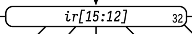
Next state would be 32 (instruction decode) stage where we are decoding which instruction is it based on the OPcode values i.e. IR bits 15, 14, 13, 12
For this course assuming some magic happens and we get correct instruction decode without any signal activations (hence this row will be emtpy in the table)
-
Lets say a magic oracle told us the next state would be 3 since we are doing store
-
Now as a practice can you break down the steps like we did in previous steps??
-
i've color coded the steps for reference, but a good excercise would be to word them out
-
-
-
Then the next state would be simply be 25
-
-
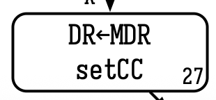
Then the next state would be 27 based on state machine
-
-
Thats' it we are done with entire instruction cycle
-
Instruction Fetch
-
(state 18 to 35) helps us fetch the 16 bit instruction 0010 111 000000001 for the current point in code using PC
-
-
Instruction Decode (magic state 32) (basically find what type of instruction to run)
-
Execution Stage (state 3) (doing the math for that instruction using either ALU or Adders)
-
Memory Stage (state 25) (loading or storing the data to memory)
-
Write Back Stage (state 27) (writing the result of that instruction either from doing math or from memory into the Destination Register DR)
-
-
This cycle happens for all instructions and thats one way of filling the reference table
Verifying Correctness
-
if u want to see if your table is correct,
-
simply draw your datapaths on the circuit and write all the signals that you would need to turn on in each state.
-
then trace the wires from state 18 to state 27 to state 18 and your tracing must be a continous line without any breakpoints
-
-
Lastly make sure to avoid breaking any common facts
Common Facts
-
LD (symbol: veritcal cross) signals are basically used when u want to write something to any registers eg- MAR, MDR, DR, CC, PC, IR, etc
-
Gate (symbol: triangle) signals are used when u want to let any data flow into the bus
-
make sure in each state atmost 1 gate is open (if u have 2 or more gate open at once in one state then its bad why??? (ponder on it)
-
-
MEM only communicates with the circuit using MAR, MDR registers and signal RW (think about the behaviour of it when RW = 1 and RW = 0)
-
M.xxxxx: represents muxes, usually used when u see a trapezium on the cirucit
-
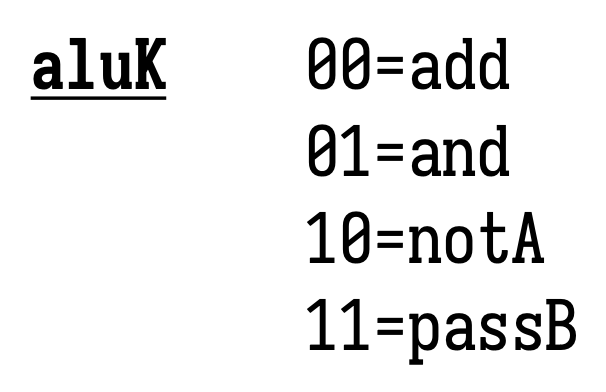
ALU: its arithmetic logic unit, it does a lot of things other than just adding, and its behaviour is controlled by aluK signal (it takes in 2 inputs A and B which can be registers or immediate values.
-

-
PassB: represents simply means do not do any math, just output the input B as it is
-
notA: simplre represents, do not do any math simply take a negation of input A
-
Note: ALU is different than PC ADDER
-
-
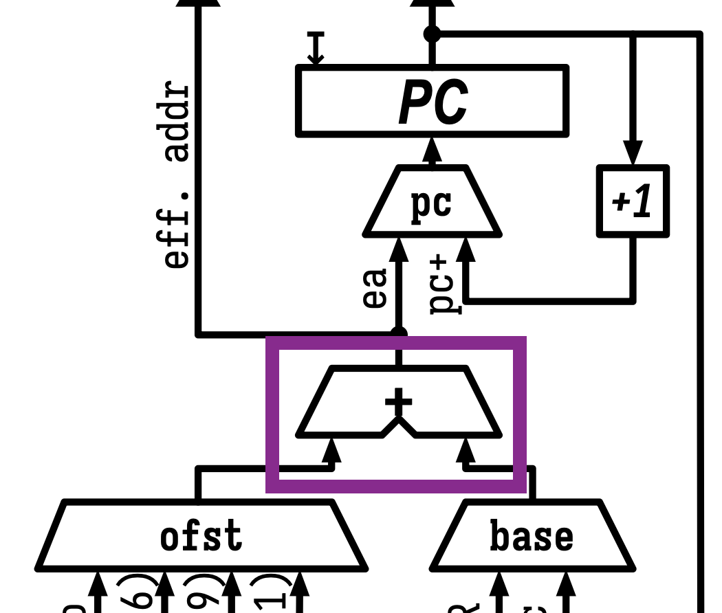
Adder:
-
This is simply a adder which adds 2 inputs (specifically offset values and base values)
-
Usually u will use them when u deal with address manipulation (like PC+offset, JMP, JSR, etc)
-
its entire reserved for doing address related computation so use this rather than using ALUk
-
-
-
Some common abbrevations:
-
SR: source register
-
baseR: base register
-
DR: destination register
-
imm5: 5 bits immediate value
-
zero: literally means a bunch of 0s
-
off9: 9 bit offset values
-
eff addr or ea: effective address
-
se(X): sign extended value of X
-
calc CC: calculate CC value with magic
-
r.out: read out, ouput of the read value from memory
-
w.in: write in, input for the value that we need to write to memory
-
mem: memory
-
bus: bus line's data
-
RW: read or write
-
aluK: Arithmetic logic unit kontrol
-
REG FILE: register file where all the registers live (Note registers lives here not in MEM)
-
MAR: Memory address register
-
MDR: Memory data register
-
IR: instruction registe (where ur single instruction lives in binary format)
-
PC: Program Counter (stores address of an instruction)
-